Nvidia Volta GPU Has 21 Billion Transistors And 5,120 Cores — “You Can’t Make A Chip Any Bigger”
Short Bytes: At its annual GTC conference, Nvidia unveiled its new Volta architecture. Based on the same, Tesla V100 data center GPU comes with whopping 21 billion transistors that deliver an equivalent performance of 100 CPUs for deep learning. Compared to the current Pascal architecture, Volta delivers 5x improvements in peak teraflops. Volta chips are expected to be used by tech giants like Google, Amazon, Facebook, Baidu, etc. in their applications.
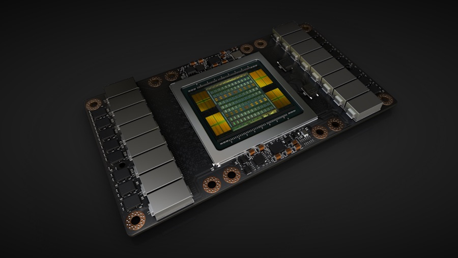
Nvidia, the market leader in computer and server graphics, has unveiled the first official Volta GPU, i.e., the Tesla V100. To make this monstrous chip, the company spent $3 billion in research and development. The company showed off this top-of-the-line product at its annual GPU Technology Conference (GTC).Volta is Nvidia’s next generation GPU architecture. While we might call Volta a GPU, it’s a lot more than that. It comes with 640 new tensor cores which can work with standard GPU CUDA cores for better performance in deep learning environments. In some way, Nvidia’s approach of accelerating the value inferring process based on a trained model is similar to Google’s Tensor Processing Unit.
Build using TSMC’s tiny 12nm production process, Tesla V100 chip contains 21 billion transistors and 5,120 CUDA cores. It reaches the peak performance of 120 teraflops. It packs 16GB HBM2 DRAM that can reach peaks speeds of 900GB/sec.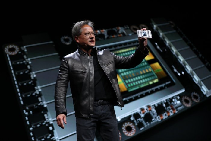
Compared to the Pascal architecture, Volta enables 5 times better performance in terms of peak teraflop; it gives 15 times performance as compared to Maxwell architecture.
Speaking at GTC, Nvidia CEO, Jen-Hsun Huang, said that one can’t make a chip any bigger as “transistors would fall on the ground.”
“To make one chip work per 12-inch wafer, I would characterize it as ‘unlikely.’ So the fact that this is manufacturable is an incredible feat,” Huang said.
Tesla V100 GPU specs and comparison with others
| Tesla V100 | Tesla P100 | GTX 1080 Ti | |
| Lithography | 12nm FinFET | 16n FinFET | 16nm FinFET |
| Transistor count | 21bn | 15bn | 12bn |
| Die size | 815mm2 | 610mm2 | 471mm2 |
| CUDA cores | 5,120 | 3,584 | 3,584 |
| Memory | 16GB HBM2 | 16GB HBM2 | 11GB GDDR5X |
| Memory bandwidth | 900GB/s | 732GB/s | 484GB/s |
Nvidia founder says that deep learn has created an insatiable demand for processing power. In future, many organizations like Amazon, Google, Microsoft, Facebook, and Baidu are planning to utilize Volta chips in their applications. The Volta architecture is bound to set a new level of computing performance on a chip and benefit the development in AI.
Did you find this story on Nvidia Volta GPU interesting? Don’t forget to share your views.
Also Read: Nvidia’s Credit Card-Sized AI Computer “Jetson TX2” Runs Linux