Factors Behind Data Backup Avoidance: Exploration
In this day and age, where people capture every moment with their smartphones, data backup and…
As our tagline “Fresh Bytes of Technology” implies, our team works tirelessly to deliver the latest updates from the tech world in a crisp and easy-to-follow format. Follow us on different social media channels as well as Google News to keep yourself updated with the latest knowhow of tech giants, security/privacy, smartphones, operating systems, and latest innovations in the field of electric vehicles and artificial intelligence.

In this day and age, where people capture every moment with their smartphones, data backup and…
Snapchat is perhaps the most popular social media platform among teenagers. Moreover, the company regularly introduces…

While most of us associate Discord with gaming, the platform has also served as a hub…

Artificial Intelligence is everywhere, be it helping us redesign our office spaces or even programming. However,…
Artificial Intelligence chatbots have taken the world by storm, be it by allowing individuals to make…

When Apple reintroduced the iPhone SE, it offered a great choice for users who wanted the…

In the post-pandemic era, it’s no surprise that monitoring health metrics has become a crucial aspect…

It’s no secret that iQOO has experienced a remarkable resurgence in recent years, transforming from a…
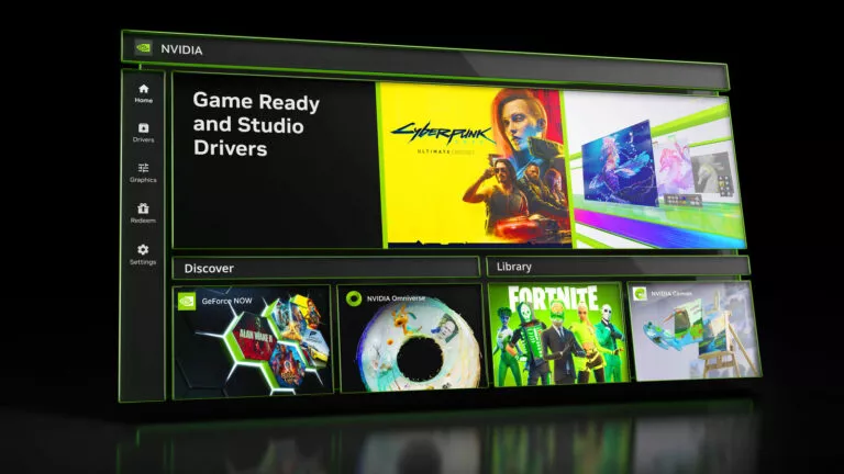
While Nvidia’s GPUs are top-of-the-line, its software for managing the performance of its cards has often…
When Google first announced the Pixel Fold, many expected the company to lead the charge in…